Tracks, channels or linear electrodes can be defined.

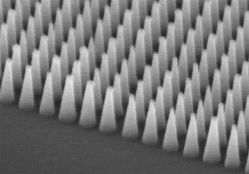
Raised dots or wells from 20 nm upwards can be formed in a variety of materials over large areas

Specialists in laser grating lithography and etch methods.


公司简介
KNT (Kelvin Nanotechnology) has been in business for over 20 years. Now an internationally recognised provider of advanced photonics and quantum components, we have built up an extensive global blue-chip customer base and provided services for 170 companies in 23 countries in three years.
We are an established comprehensive photonic fabrication service provider for diverse market sectors and a qualified supply chain partner for multiple global product lines.
As one of the first suppliers of miniaturised quantum components in the market, we produce 3D ion traps, grating MOTs, MEMS gravimeters and specialist DFB lasers for international partners and customers. We are driving forward innovation in fabrication of quantum components to support quantum systems for information processing and computing, chip scale cold atom systems, sensors and high precision timing and navigation.
We provide early prototype and proof of concept support to research and industrial organisations. We’re process driven, and have a customer focused culture that successfully transforms ideas into reality.
产品列表
KNT has been a key supplier in the photonics sector for over 20 years, delivering advanced services and products to a global customer base. Quality is at the heart of everything that we do, allowing us to achieve qualified partner status for multiple international supply chains.
We have expertise in processing materials such as indium phosphide, gallium arsenide, silicon, silica etc. used in common optical devices. These are applied to a host of devices such as miniature lasers for portable quantum technologies and datacoms; light engines for near-eye and head up display systems used in augmented reality applications; and photonic interconnects such as waveguides, multiplexers, couplers and modulators.
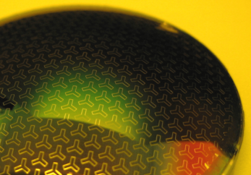
Surface optical structures such as Diffractive Optical Elements (DOEs), photonic crystals, plasmonic filters and anti-reflective surfaces have also been produced using our advanced lithography and complementary processes.
Specialists in laser grating lithography and etch methods.
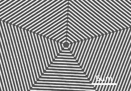
Two-dimensional photonic-bandgap structures.
Biomimetic anti-reflective coatings for numerous applications.
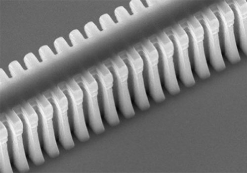
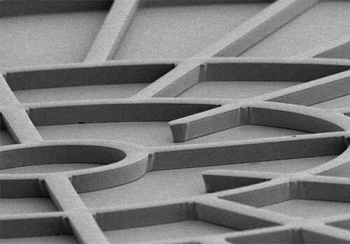
Kelvin Nanotechnology has over twenty years’ experience in electron beam lithography and nanofabrication. Electron beam lithography provides a route to versatile nano-patterning for a vast range of applications. Single or multi-level patterns can be written onto almost any type of substrate then transferred by etching or depositing metals, insulators, biocompatible materials, optical or electronic layers.
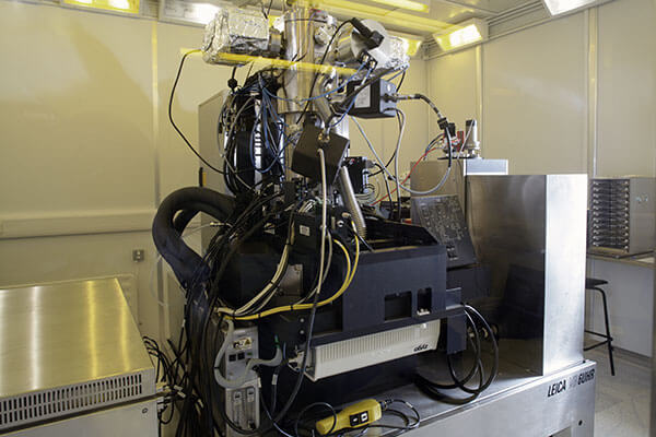
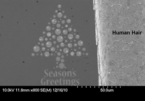
Our core technology is based around an electron beam lithography suite containing Nanobeam nB5 and Raith EBPG5200 commercial tools. Features from 20 nm can be written easily and quickly on up to 200 mm wafers. Full industrial service contracts ensure 96% up time and with over 50,000 samples written in the last ten years, this high utility translates into cost effective manufacturing.
We specialise in high resolution, large area, multi-level electron beam lithography for photonics, quantum technologies and telecoms industries. Applications include devices such as laser gratings, transistor gates, imprint masks, optical elements, photonic crystals, nanotextured surfaces and many more.
This depth of experience at KNT is central to our ability to translate your needs to high resolution patterning.
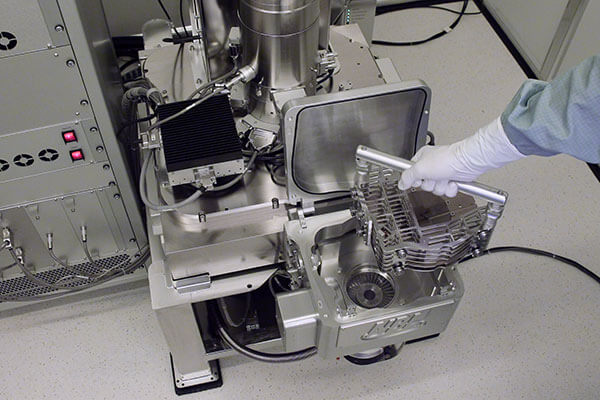
We provide cost effective nanolithography with a 24-7 operation across three commercial EBL tools working at nm to mm length scales.
‘Pure-play’ E-Beam Foundry – customer supplied designs produced on a variety of substrate materials.
High resolution – feature sizes start at 20 nm with the capability to form sub-10 nm nanogaps.
Large area writing – cm sized patterns
Multi-level processing – level to level registration better than 15 nm (standard) or 1 nm (special) achieved using custom marker recognition software.
High throughput – rapid load/unload process by team of technicians has enabled >50,000 wafers written in last 10 years.
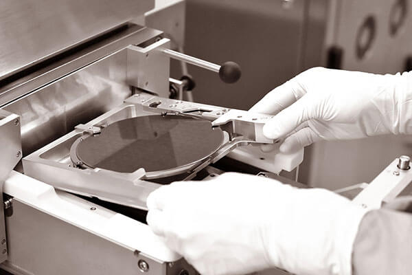
Up to 200mm diameter wafers – cassette exchange system enables multiple wafers to be written sequentially.
Extensive process database – covering the processing of semiconductors, dielectrics, metals and polymers.
Excellent cost-to-yield – from process setup and optimisation to Live wafer writing.
Application expertise – multi-discipline technical team with over 20 years’ experience spanning semiconductor, optoelectronics, nanoelectronics, quantum and bioelectronics sectors.
Tracks, channels or linear electrodes can be defined.
Raised dots or wells from 20 nm upwards can be formed in a variety of materials over large areas
Specialists in laser grating lithography and etch methods.

3D lithography used for wafer scale fabricated scanning thermal probes capable of resolving 0.1 mK temperature changes with 100 nm spatial resolution.

Compact, easily configured approach to cooling atoms in a magneto optical trap.

Two-dimensional photonic-bandgap structures.
Proof of concept, feasibility studies and prototyping projects cover a broad range of technical areas, complexity and duration; and form an important part of our business. We help companies of all sizes to realise their ideas and innovations. Working with us, we can understand your device requirements to provide a defined plan of work and manage the project to deliver your goals.
We offer wide ranging R&D and prototyping services for the semiconductor, optoelectronic, bioelectronic and nanoelectronic market places.
We are constantly expanding and developing our processes and technology. We are keen to learn about your applications and technical challenges and how we might use our expertise and experience to satisfy your micro and nanofabrication needs.
The scope of a development project will be tailored according to the fabrication complexity and client time constraints. We offer a flexible service that can provide either access to individual process steps or full project and technical management.
Clean energy sector devices to enhance light harvesting.
Novel fabrication methods developed with partner organisations to provide imaging sensor.
Amplitude and phase DOEs can be produced over large areas.

Taking your initial concept to produce multi-level device lithography design files tailored to the process flow.
Wavelength selective optical filtering and enhancement.
Biomimetic anti-reflective coatings for numerous applications.
KNT are a globally recognised supplier of quantum devices and components. The fabrication of these complex devices is underpinned by our breadth and expertise in processing different materials across a range of dimensions from tens of nanometres upwards.
The components currently within our portfolio include the following:
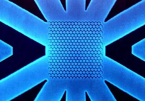
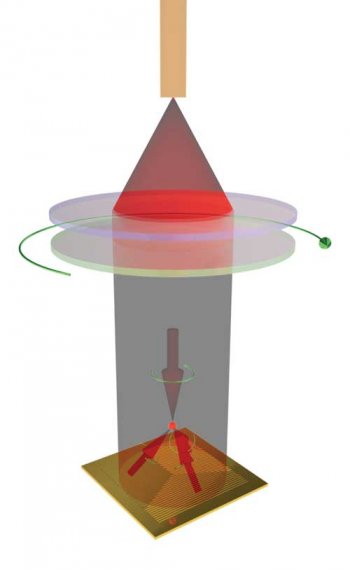
A Diffractive Optical Element that improves ease of alignment, setup and miniaturisation for cold atom source creation compared to conventional 6-beam MOTs.
The technology requires only a single laser beam and can be used inside or external to the vapour cell; making the flexibility of quick change cold atom experiments possible. The grating MOT (gMOT) has gained much interest from the Quantum Technology community and is envisaged to become the heart of quantum systems utilising cold atoms for timing and sensing applications.
This work was published in Nature Nanotechnology.
Performance
Trapping over 10 million 87Rb atoms
Cooling below 40 µK
Atom Clouds denser than 1010/cm3
Application
Central to quantum technology research.
Simplification
Enables laser cooling with a single laser beam while significantly reducing the overall system volume, optical access requirements, apparatus complexity and cost.
Adaptable
Can operate either inside the vapour chamber or externally through a suitable window.
Validation
Each chip supplied with actual atom number and cooling data.
This work was published in Nature Nanotechnology.
Performance Specifications
Loading rate of atoms into the MOT – >5×10⁶ /sec
Steady state number of atoms in MOT – ~107
Temperature – 3 µK to 40 µK
Density – >1010 /cm3
Chip Physical Specifications
Dimensions: 22 x 22 x 0.5 mm
Grating region: 20 x 20 mm
Material coating: Aluminium
Chip material: Silicon
Weight: 0.6 g
Input Laser Beam Requirements
Wavelength: 780.24 nm
Frequency detuning: ~12 MHz
Power: ~50 mW
Polarisation: Circular polarised (Stokes parameter |S3|≥0.9)
Collimation: Divergence angle, |θ|≤0.1o
Incident angle: Normal +/- 1o
Beam size radius: 1/e2 radius ~17 mm
Vacuum and Magnetic Requirements
Base pressure: <1 x 10⁻⁹ mbar
Rb partial pressure: <5 x 10⁻⁹ mbar
Magnetic field: Quadrupole coils aligned with chip. Axial gradient of 0.1 T/m
Ambient DC field: ≤10 µT
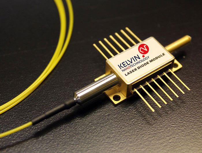
We have developed the fabrication process for narrow line width 780 nm DFB lasers for trapping and cooling of atoms e.g. Rubidium within a vapour source for the generation of Bose Einstein Condensates down to temperatures in the microkelvin regime.
These lasers will be utilised for atom cooling and interrogation for quantum enabled precision timing and sensing applications.
These 3D micromachined ion traps enable the trapping of multiple ions and will form the foundations of future quantum computers. They were first reported by NPL in the journal Nature Nanotechnology and are now produced at the wafer scale by KNT. This wafer-scale process was co-developed with NPL and Optocap.
The animation shows the fabrication process – 1) definition of surface electrodes, 2) deep SiO2 etch, 3) Ohmic electrode formation, 4) Silicon etch to form cavity, 5) internal electrode metallisation and 6) thickening of electrodes.
Microfabrication of ion traps ensures reproducibility of device dimensions, scalable manufacture and supply.
A MEMS technology that is complementary to quantum gravimeters enabling a reference, low power, no need for calibration, deployable, sensitive device. The process approach permits device performance (sensitivity, frequency) to be readily tuned to the application. It can be used to measure small variations in density underground to create gravity images valuable in fields such as energy, civil engineering, defence and environmental monitoring. Devices could also be used to survey geophysical explorations using drones instead of plane or alternatively networks of gravimeters could be positioned around volcanoes to monitor the intrusion of magma that occurs before eruption – acting as an early warning system.
This technology was reported in the journal Nature demonstrating its use in the measurements of earth tides.